Two weeks ago, the tech world celebrated the 50th anniversary of Moore’s Law — Intel cofounder Gordon Moore’s tenet that transistors per chip would roughly double every two years. For several decades, analysts have wrongly predicted the end of Moore’s Law, only to see it bounce back like Flubber. The end does indeed appear to be coming, but probably not for at least 10 years, according to Intel Senior Fellow Mark Bohr, quoted in a recent PC Mag article.
Even if the upcoming shift to 10-nanometer, 7 nm, or possibly 4 nm, processes finally push up against the limits of semiconductor miniaturization, semiconductors will likely continue to grow more varied and adaptable, while gaining more human-like neural processing capabilities. Last month, for example, Qualcomm announced an emerging cognitive computing technology called Zeroth, which it intends to start baking into future Snapdragon system-on-chips.
Meanwhile, more iterative advances continue to change how we use processors and the increasingly complex, multi-core SoCs built around them. Here’s a brief look at some Linux- and Android-related chip highlights culled from only the last few weeks: an open MIPS core for academics, new Cortex-A72 details, MediaTek’s deca-core Helio X20 SoC, and TI’s new DSP-fueled FPGA competitor.
Imagination releases Linux-ready open MIPS core for academics
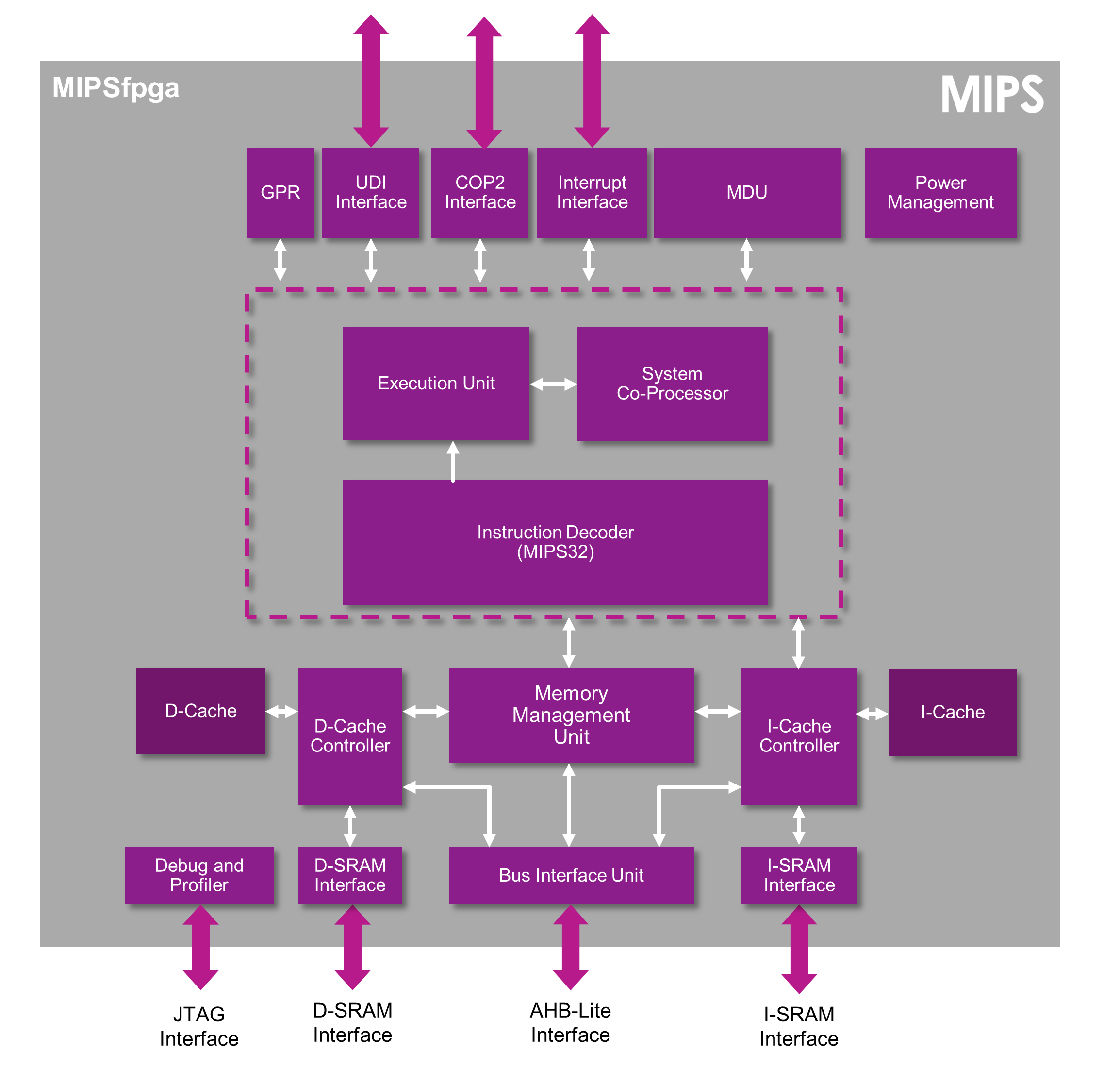
Imagination Technologies gets a bad rap in the open source world for selling one of the most closed proprietary graphics co-processors around. (If PowerVR wasn’t so good, we wouldn’t complain so much.) Yet the MIPS architecture it acquired a few years ago has always been one of the more open, or at least well documented, of the major computing platforms.  Imagination is continuing the tradition by releasing a special free and transparent version of its 32-bit MicroAptiv processor called MIPSfpga.
Starting in May, MIPSfpga will be available to academic institutions as a fully visible RTL design that can run on FPGAs. It’s free and open, but not fully open source. Researchers can see deep into the design and modify it at will, but cannot implement it in silicon or establish patents based on it without an agreement.
The device is more like a microcontroller than a full application processor, but you can run Linux on it. The final Linux code will take a few more months, however.
MIPS is popular in computer research and education due in part to its substantial documentation, as well as its “true RISC” attributes. By comparison, ARM and x86 have morphed a lot more over the years from their RISC roots. However, the lack of a highly visible working MIPS model has been a challenge for educators.
MIPSfpga is more simplified than MicroAptiv, and it modifies the MIPS load/store architecture with a more elegant “instruction bonding” technology, but otherwise stays close to its roots. The chip design ships with FPGA implementation guides and teaching materials. More information and sign-up for access may be found at Imagination’s website.
In another MIPS-related open source development this week, Cavium, which builds MIPS-based Octeon III processors for high-end networking and storage applications, announced that its lower-end, MIPS64-based CN70/71XX versions of its Octeon III SoCs will ship with a free, open source OpenWRT Linux distribution. Designed for consumer/SMB routers and security appliances, the SoCs also support commercial, carrier-grade Linux distros including Wind River Linux and Cavium’s own MontaVista Linux. However, the optimized, lightweight OpenWRT distribution can open up more resources for enterprise applications, says Cavium.
Meanwhile, a fully open source RISC design called RISC-V is progressing at UC Berkeley, along with an associated lowRISC project that plans to build an open source SoC and hacker board to run it. The lowRISC project just released its first preview version of the Linux-oriented SoC design, which demonstrates support for tagged memory.
ARM borrows from the future for Cortex-A72
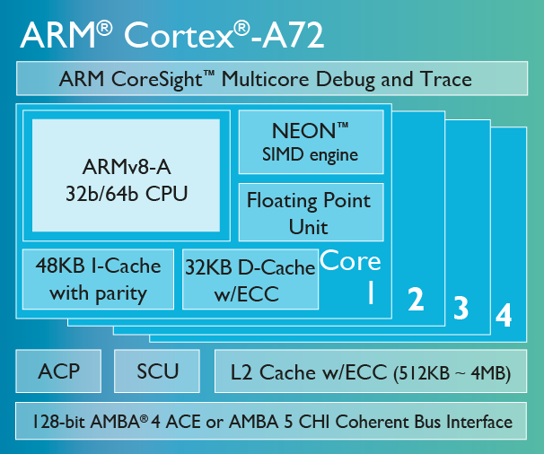
 ARM unveiled its Cortex-A72 processor design in February with claims that it is twice as fast as the similarly 64-bit Cortex-A57. Last week, ARM revealed more details about the -A72 at the Linley Mobile Conference. According to Embedded.com, Brian Jeff, director of marketing for ARM’s Cortex-A products, revealed that the Cortex-A72 includes three functional units “borrowed” from an unannounced future core: a branch-predict unit, a load/store unit, and a floating point unit (FPU).
Jeff is quoted as saying the new branch predictor significantly reduces cache misses, and the load/store unit decodes micro-operations at later stages in the pipeline in order to “get more throughput in the front end and save decode power.” The FPU, meanwhile, lowers latency by as much as 50 percent for some operations. While these components are tuned toward power efficiency on the -A72, they can also be configured for more performance. Embedded.com interpreted several comments by Jeff to suggest the future “enterprise” chip design will do just that in an attempt to catch up to Intel’s x86 chips on their relative strength: sheer performance.
MediaTek’s 10-core Helio X20
MediaTek, which is shaping up as a major competitor to Samsung, Qualcomm, and Nvidia in the market for mobile SoCs that drive the Android world, has already begun sampling the first Cortex-A72 SoC with its MT8173 design. The MT8173, which features dual 2.4GHz Cortex-A72 cores and dual Cortex-A53 cores, should appear in tablets later this year.
There’s even greater interest in MediaTek’s MT6797 Helio X20, a more recently revealed SoC design that also uses Cortex-A72 cores. The Helio X20 is said to be the first 10-core (deca-core) SoC, and the first with a new Tri-Cluster CPU architecture designed to replace ARM’s Big.Little heterogeneous multi-core technology. The SoC will combine two 2.5 GHz -A72 cores with four 2.0 GHz –A53 cores and four 1.4 GHz -A53 cores.
This Tri-Cluster design adds a “medium” performance/efficiency tradeoff. In addition to optimizing the -A72 cores for speed and the 1.4GHz -A53 cores for efficiency, you can run mid-level routines with the faster -A53 cores. This week Digitimes reported that the Helio X20 will use TSMC’s 20 nm process. ARM previously announced that homogeneous Cortex-A72 designs will be able to move to TSMC’s new 16nm FinFET+ node fabrication process. By comparison, Intel has already moved to 14 nm with its new Broadwell and Cherry Trail chips.
TI SoC takes on FPGAs in data acquisition
Years ago, Texas Instruments stepped back from the limelight — and cut-throat competition — of the mobile world to focus solely on embedded. For much longer, however, it has been fighting a war to pitch its digital signal processors (DSPs) as alternatives to field programmable gate arrays (FPGAs) from companies like Altera and Xilinx. Last week, TI unveiled a 66AK2L06 SoC that uses a combination of Linux-driven Cortex-A15 cores and DSPs to compete directly with FPGAs in data acquisition (DAQ) applications used in avionics, defense, medical, and test and measurement equipment.
The 66AK2L06 is related to its Linux-ready, DSP-enabled Keystone II SoCs, but adds two major new features that help it compete with FPGAs in the DAQ market. The first is a Digital Front End (DFE), which offers features like a Digital Down Converter / Up Converter (DDUC), an NCO/mixer, functional resampling, and noise and image filtering and shaping. There’s also an interface compliant with the JESD204B serial standard, which is supported by a variety of TI’s analog-to-digital converters (ADCs), digital-to-analog converters (DACs), and analog front ends (AFEs).
The bottom line, according to TI is that the 66AK2L06 can do almost everything FPGAs can do in data acquisition, but can do it in a way that is cheaper, faster, and more power efficient. The SoC is also claimed to be easier to work with than using FPGAs.


